
This post is part of a series in which I am following the structure of J. Clark Scott’s book But How Do It Know? (Affiliate Link – commission supports my knowledge quest). You can check out his website at http://www.buthowdoitknow.com/ (not an affiliate link). It’s written with no assumption of knowledge or background in computers, which has been great for me 😉
What Do Logic Gates Actually Look Like?
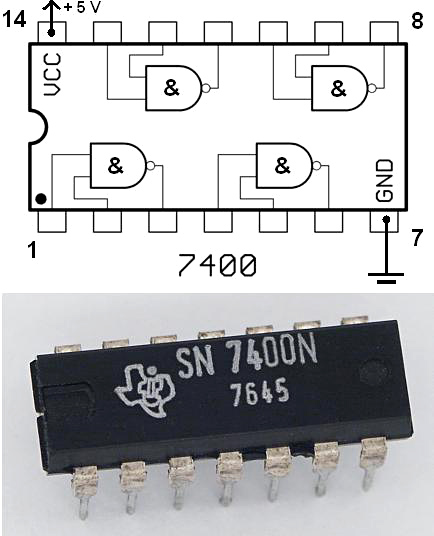
A computer is essentially a rat’s nest of fairly straightforward contraptions called logic gates. The two components that make a computer a computer are full of them – the CPU and RAM (See link for my post on how they communicate). They operate using electrical wires (turning them on and off to represent 1’s and 0’s) that serve as “input” (going into the gate) and “output” (coming out of the gate). There are lots of circuit diagrams out there that use symbols, but it’s kind of tough to get a look at what a logic gate might physically look like. The best photo I could find of a real device was actually here on Wikipedia (where all good things come from) on the page for NAND gate. I like it because it juxtaposes the symbol diagram alongside the actual chip. (There was no attribution information for this photo, please let me know if you find it. I’d be more than glad to give credit where it’s due)

J. Clark Scott’s book purposefully avoids talking about the physical construction of such devices, as it’s outside of the scope of the discussion of logic. Since you can’t really see anything that actually shows the internal workings of the 7400 chip shown above, perhaps the next best thing is a really amazing YouTube video on a computer constructed inside Minecraft (a computer game focused on building stuff with blocks, in case you’re not familiar). My hat’s off to the creator, I’m in awe of his creation. In any case, suffice it to say that logic gates are constructed by some physical medium using using chemistry and physics that I don’t yet understand. For now, at least, that awesome YouTube video will have to do.
Universal Gates
What struck me in learning about logic gates was that a number of gates are actually just combinations of other gates. There seems to be a bit of confusion out there on various sites regarding what gates are used to construct what gates, but the general consensus seems to be that NAND (negative-AND) and NOR (negative-OR) are the universal building blocks to build other gates, especially ones that are a little easier to understand like AND, OR, and NOT. In any case, most places purport the existence 7 gates (AND, OR, NOT, NAND, NOR, XOR, XNOR), but the best site I found was an article at All About Circuits on logic gates that shows a total of 16 (although some of them aren’t really gates or binary).
The reason why NAND and NOR are used to build everything else seems to be that the are easily built physically. If I understood more about chemistry and physics I could probably give you a more specific reason based on physical and chemical properties, but most descriptions I can find just say that you need to trust that NAND and NOR are built, then the rest are assembled with multiple interconnected NAND and NOR gates. For example, I have an AND implementation using two NAND gates shown below:
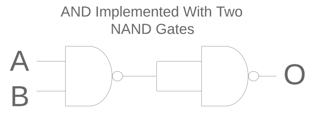
This contraption will turn O on only if both A and B are turned on, just like an AND gate.
How Does It All Fit Together?
Another shameless plug for J. Clark Scott’s book But How Do It Know? (Affiliate Link – commission supports my knowledge quest) because he does a really good job explaining how you would put these gates together to store 8 bits, which is also called a byte. Typically the register size is the size of the CPU’s computational “width”. Nowadays most CPU’s 64 bit, so their registers would be 64 bit as well, although in some cases there may be smaller ones. This tutorial on howstuffworks.com also does a good job explaining registers (didn’t like the section on the gates themselves though, heads up), and uses some terminology that you’ll definitely come across looking at logic gates, such as flip-flop and feedback. Storing a collection of on or off bits into a collection of fancily interconnected logic gates using a “set” wire as input allows you to store the state of the bits when the set wire was activated. Another wire, called “enable” allows you to access or read the bits. Such a collection is called a register, allows you to write bytes and read bytes. Amazing.
You’ll see registers all over the place, usually with a word or words before it to specify what its purpose is, such as Memory Address Register that says you want to access a certain address in memory and transfer the contents stored there (also in a register, called a Memory Data Register) to the CPU, where it will likely store said contents temporarily in a CPU register. All of the actions I have described are executed using combinations these gates, using voltage rising and falling as signalling to represent 1’s and 0’s across the wires. Some of the circuit diagrams and logical collections of gates in modern boards, memory and CPU’s can be intimidating, but I just try remember back to how simple the gates themselves are, and it makes me feel better.